PCI - Peripheral Component Interconnect

All signals except Reset, Interrupt are sampled at rising edge of clock.

Operation:

A bus transaction is followed by an address phase followed by one or more data phases. Address phase starts when FRAME# is asserted. For read operation TRDY#(target ready) is asserted. For write operation IRDY#(initiator ready) is asserted. Data phase completes on any clock both IRDY#, TRDY# are asserted. Wait cycles are inserted until both are asserted together.

Address, Data pins are multiplexed. C/BE# pins are multiplexed. They define bus command for address phase, byte enable for data phase. STOP# signal indicates the current target is requesting the master to stop the current transaction. LOCK# used for atomic operations. IDSEL (Initialization Device select) used as chip select for configuration read, write transactions. DEVSEL# indicates whether any device on the bus is selected. Arbitration signals (REQ#, GNT#) of bus master: request, grant access to bus provided RST# is de-asserted.

PAR – even parity signal; has same timing of address/data but delayed by one clock. PAR is driven by master for address, write data phases, and by slave for read data phases. PERR#, SERR# report data parity error, system error(address/command) respectively.

M66EN indicates 33MHz or 66MHz. ACK64# acknowledges 64 bit transfer.

Optional Signals:

INTA#, INTB#, INTC#, INTD# -- request interrupt. PRSNT indicates the motherboard presence of add-in board. CLKRUN# indicates status of CLK. PME -- asynchronous signal used to request a change is system power state. 3.3VAUX -- auxiliary power source. TCK, TDI, TDO, TMS, TRST# -- JTAG signals

OSI Reference Model


Application Layer: End user processes like file transfer, e-mail, network software services. E.g. Telnet, FTP

Presentation/Syntax Layer: Format, Encrypt data to send across network.

Session Layer: Establishes, manages and terminates connections between applications .

Transport Layer: End-to-end error recovery, flow control.

Network Layer: Switching, Routing, Addressing, internetworking, error handling, congestion control and packet sequencing.

Data Link Layer: Encoding, decoding data packets into bits.

Media Access Control Sub-layer: Data access/transmit permissions.

Logical Link Sub-layer: Frame synchronization, flow control, error checking.

Physical Layer: Conveys the bit stream (electrical, light, radio)
E.g. Ethernet, RS232, ATM

SPI Interface

The SPI-bus is a 4-wire serial communications interface used by many microprocessor peripheral chips. The Serial Peripheral Interface (SPI) circuit is a synchronous serial data link that is standard across many Motorola microprocessors and other peripheral chips. It provides support for a low/medium bandwidth (1 megabaud) network connection amongst CPUs and other devices supporting the SPI.

SPI bus is basically a relatively simple synchronous serial interface for connecting low speed external devices using quite minimal number of wires. SPI (serial peripheral interface) is an interface standard defined by Motorola on the MC68HCxx line of microcontrollers. A synchronous clock shifts serial data into and out of the microcontrollers in blocks of 8 bits. SPI - Serial Peripheral Interface. SPI is used frequently in handheld and other mobile platform systems.

SPI bus is a master/slave interface. Whenever two devices communicate, one is referred to as the "master" and the other as the "slave" device. The master drives the serial clock. When using SPI, data is simultaneously transmitted and received, making it a full-duplexed protocol.

Motorola's names for the signals are as follows: SCLK for serial clock, which is always driven by the master: MISO is master-in slave-out data: MOSI is master-out slave-in data. In a typical application, connect the microcontroller's SCLK to the converter's SCLK input, connect the MISO to the converter's DOUT pin, and connect the MOSI pin to the converter's DIN pin. Serial protocols such as SPI, a chip-select input is required to enable the IC. Using this chip-select signal it is possible to connect many ICs to same SPI bus in parallel. If there is a chip-select (CS) signal in use, it can be driven by a spare microcontroller general-purpose output. Every IC connected to bus needs it's own chip-select signal line. Thus, when 10 devices are on the bus, 10 chip-select lines, in addition to the shared clock and data lines, are needed to select the appropriate device.


The SPI interface is based on a 8 bit shift register. The shift clock (SCK) is provided by the master device. SCK is a gated clock and is only generated during shifting. SCK stays idle between transfers. Transmitting and receiving occurs simultaneously: While the master shifts out it's transmit data, data from the slave is shifted in. As a result, the master must always send data in order to generate clocks, even if only data reception is required. The following diagram shows a basic interface and a sample data transfer: Data on SDO is shifted out with the falling SCK edge; data on SDI is sampled on the rising SCK edge. The SCK idle polarity is 'High'.


Einstein's Quote


Make one like this one here

http://www.hetemeel.com/einsteinform.php


Eye Diagram


By super-imposing the transition patterns of a signal for 011, 001, 100, 110,
we get an Eye-Diagram. This is used to study Jitter, Voltage swing and Transition time.
The above diagram shows perfect one, practical one respectively.

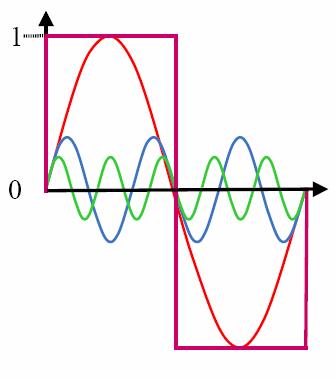
Harmonics


Legend: Signal

Dark red : Square wave of amplitude 1

Light red: sin wt

Blue : (1/3)sin 3wt Third Harmonic

Green : (1/5)sin 5wt Fifth Harmonic

Transmission Lines

Transverse Electromagnetic Waves: Propagation of energy in a transmission line takes place such that electric and magnetic fields transverse to one another and also to direction of propagation. The resultant wave is termed as TEM wave.

Consider a small section n of a parallel wire.
Length of this line is dx.
Voltage at input is V, at the other end is V+dV; Similarly current is I, I+dI.
Assume Primary Line Constants of the line are R,L,G and C
Note: w= 2.pi.f

For small dx, dI is zero.
Potential drop across the line is V – (V+dV) = R.dx.I + jwL.dx.I
 -V’ = I(R+jwL) ….. eq.1
Note: V’ = (d/dx)V

In a similar method, assuming dV is zero,
 -I’ = V(G+iwC) ….. eq.2

Differentiate eq.1,2
V”= V(R+jwL)(G+jwC) ….. eq.3
I” = I(R+jwL)(G+jwC) …..eq.4

Let (gamma)^2 = (R+jwL)(G+jwC)
Gamma = (alpha) + j(beta)

alpha is attenuation constant
beta is phase constant
gamma is propagation constant

Now eq.3,4 becomes
V” = V. (gamma)^2
I” = I. (gamma)^2

Solving the above equations,
V=A.exp(-gamma.x) + B.exp(gamma.x) …..eq.5
I= C.exp(-gamma.x) + D.exp(gamma.x) …..eq.6
Note: exp(x) = e^x

The first terms in eq.5,6 are called incident component(magnitude of V or I decreases from source towards load, whereas the second terms are called reflected component(magnitude of V or I decreases form load towards source)

Hypothetical infinite line: Voltage at distant end approaches zero(i.e no reflected component)

At x=0, V=Vs
Substitute in eq.5, Vs=A+B
At x=infinity, V=0
 B=0, V= Vs.exp(-gamma.x)
V’=-gamma.Vs.exp(-gamma.x)=-(R+jwL)I
Simplifying,
I=(Vs.exp(-gamma.x))/Z0
Where Z0=[(R+jwL)/(G+jwC)]^(1/2)

Z0 the input impedance of such infinite line is commonly referred to as Characteristic Impedance of the line. Z0 and propagation constant are termed as secondary constants (or coefficients) of the line


Line Terminated in a Load Impedance Zr:
At a distance x from the source, voltage and current are Vx, Ix.
-V’=(R+jwL).Ix
Substitute the above after differentiating eq.5,6 and then simplifying,
Voltage, current at source are Vs=A+B, Is=(A-B)/Z0
Vx=Vs.cosh(gamma.x)-Is.Z0.sinh(gamma.x) …..eq.7
Ix=Is.cosh(gamma.x)-(Vs/Z0)sinh(gamma.x) …..eq.8

For load impedance Zr, length of transmission line is l.
Ix=Ir, Vx=Vr such that Vr=Ir.Zr

Substitute the above in eq.7,8, and solve for Vs/Is
Input Impedance Zin = Vs/Is = Z0.N/D
Where N = Zr.cosh(gamma.l) + Z0.sinh(gamma.l)
D= Z0.cosh(gamma.l) + Zr.sinh(gamma.l)

Line Terminated in Load Impedance Z0:
Zr=Z0 in N,D
 Zin=Z0

A line terminated in its characteristic impedance has input impedance equal to Z0. In such a line, there is no reflected component and at any point x distant from the signal source, the voltage and current are same as that for infinite length transmission line.

Low frequency transmission line:
R is very bigger than wL
G is very lesser than wC
Z0 = (R/jwC)^(1/2)

High frequency line:
R is very lesser than wL
G is very lesser than wC
Z0 = (L/C)^(1/2)

Cross Talk

Cross Talk: Interference between signal lines
Z0=[(R+jwL)/(G+jwC)]^(1/2)
At high frequencies, capacitive reactance increases, it leads to reduced Z0
As the length of transmission line increases, it leads to increased inductive reactance, consequently reduced Z0.
If the line impedance is low, the series impedance as seen by the induced voltage is low, allowing large induced currents to flow. Thus crosstalk is generated from both capacitive and inductive coupling between signal lines

Differential/Balanced transmission

A pair of signal lines(true and inverted) is essential for each channel (there is additional ground return path). Noise is coupled to both wires of the pair, hence rejected by common mode rejection capability of differential amplifier.
Ground noise is also rejected by common mode rejection capability.

Voltage levels for various bus standards

Signal type

Standard

VCC

VOH

VIH

Vt

VIL

VOL

Single Ended

5V CMOS

4.5-5.5

VCC-0.2

0.7 VCC

2.5

0.3 VCC

0.5

2.5V CMOS

2.3-2.7

VCC-0.2

0.7 VCC

1.25

0.2 VCC

0.2

3.3V CMOS

LVTTL

3.0-3.6

2.4

2.0

1.5

0.8

0.4

5V TTL

4.5-5.5

2.4

2.0

1.5

0.8

0.4

ETL

4.5-5.5

2.4

1.6

1.5

1.4

0.6

GTL


1.2

0.85

0.8

0.75

0.4

GTLP


1.5

1.05

1

0.95

0.55

TIA/EIA-232-F

RS-232


5

3

0

-3

-5

Differential

Standard

VDD

VOH

VIH

Vdiff

VIL

VOL

SSTL_3 Class I

3.3

2.1

1.9

0.4

1.1

0.9

SSTL-3 Class II

3.3

2.3

1.9

0.4

1.1

0.7

SSTL_2 Class I

2.5

1.82

1.7

0.35

0.8

0.68

SSTL_2 Class II

2.5

2.01

1.7

0.35

0.8

0.49

USB

4.5-5.5

3.0-3.6


2.0

0.2

1.3


T1A/E1A -644

RS-644

LVDS

2.4

1.32

1.25

Vt=1.2

1.15

1.07

Single-ended transmission

Single-ended transmission is performed on one signal line, and the logical state is interpreted with respect to ground. Twisted pair cable recommended for distance more than 1 metre. E.g. EIA232
The poor noise immunity limits the distance and speed of reliable operation.

Calculation of Characteristic Impedance for given IO standard

Consider 3.3V CMOS, that provides drive capability of 24mA
Max value of VCC is 3.6V.
VOH is 2.4V.
Maximum allowed drop in the transmission line for proper operation is
VCCmax – VOH = 1.2V.
 Maximum allowed impedance of the line is 1.2/0.024 = 50 ohms

Data Transmission Topologies

Point-to-point: One transmitter, one receiver per line
Multi-drop: One transmitter, many receivers per line
Multi-point: Many transceivers per line

DDR2 SDRAM differential strobe

When DQS# is disabled (bit E10=1), the data strobe operates in single ended mode similar to DDR SDRAM

VME protocol

The master puts address onto the bus, delays a minimum of 35ns, and then asserts address strobe. All slave cards on the bus monitor the addresses. Each slave is set up to decode a unique address. For a write operation, the master asserts one or both of its data strobes. The assertion of data strobe tells the slave that data is valid on the bus and can be strobed into memory. The slave then asserts data acknowledge to signal that the data has been captured.

SDRAM Calculation of capacity

Calculate the number of addressable locations (don’t think of bit/byte/word for now)
Number of address lines: 11 (A0-A10)
Number of banks : 2 (BA0-BA1)
Max number of rows = 11 (i.e., no. of address lines)
Max number of columns = 11 (i.e., no. of address lines)
Total locations in a bank = 211 x 211
Total locations in the chip = (No. of banks) x (Total locations in a bank)
= 22 x 211 x 211
= 224
Organization: x4, x8, x16
Look for the min possible organization, i.e. x4
Max capacity of the chip is 224 x4 = 226 bits

Characteristic Impedance of Micro-strip line

Z0=[L/C]^(1/2)= 377(h/w)[Er^{-1/2)]
Er=Relative permittivity of the dielectric material
h = thickness of dielectric
w = trace width

Gmail Trick

When you give your email address to a website, you hope that they don't sell or trade your address to a bunch of spammers. Well if they do, here is a simple way to see what sites are responsible for what particular piece of email. This requires you have a Gmail account.

If your Gmail login name was username@gmail.com and you went to samplesite.com to fill out a registration form, instead of just entering username@gmail.com as your email, enter it as username+samplesitecom@gmail.com instead. When Gmail sees a "+" in an email address, it uses all the characters to the left of the plus sign to know who to send it to. In this example it would still send it to username@gmail.com.

Now whats cool is if you search Gmail for username+samplesitecom, you will see all massages that were sent to that email address.

To see who is responsible for sending a specific message click the Show Details link and you will see the complete address.

Heart Attack

Let's say it's 6.15p m and you're going home (alone of

course), after an unusually hard day on the job.

You're really tired, upset and frustrated.

Suddenly you start experiencing severe pain in your

chest that starts to adiate out into your arm and up

into your jaw. You are only about five miles from the

hospital nearest your home. Unfortunately you don't

know if you'll be able to make it that far. You have

been trained in CPR, but the guy that taught the

course did not tell you how to perform it on yourself.

HOW TO SURVIVE A HEART ATTACK WHEN ALONE

Since many people are alone when they suffer a heart

attack, without help,the person whose heart is beating

improperly and who begins to feel faint, has only

about 10 seconds left before losing consciousness.

However,these victims can help themselves by coughing

repeatedly and very vigorously. A deep breath should

be taken before each cough, and the cough must be deep

and prolonged, as when producing sputum from deep

inside the chest.

A breath and a cough must be repeated about every two

seconds without let-up until help arrives, or until

the heart is felt to be beating normally again.

Deep breaths get oxygen into the lungs and coughing

movements squeeze the heart and keep the blood

circulating. The squeezing pressure on the heart also

helps it regain normal rhythm. In this way, heart

attack victims can get to a hospital. Tell as many

other people as possible about this. It could save

their lives!!Let's say it's 6.15p m and you're going home (alone of

course), after an unusually hard day on the job.

You're really tired, upset and frustrated.

Suddenly you start experiencing severe pain in your

chest that starts to adiate out into your arm and up

into your jaw. You are only about five miles from the

hospital nearest your home. Unfortunately you don't

know if you'll be able to make it that far. You have

been trained in CPR, but the guy that taught the

course did not tell you how to perform it on yourself.

HOW TO SURVIVE A HEART ATTACK WHEN ALONE

Since many people are alone when they suffer a heart

attack, without help,the person whose heart is beating

improperly and who begins to feel faint, has only

about 10 seconds left before losing consciousness.

However,these victims can help themselves by coughing

repeatedly and very vigorously. A deep breath should

be taken before each cough, and the cough must be deep

and prolonged, as when producing sputum from deep

inside the chest.

A breath and a cough must be repeated about every two

seconds without let-up until help arrives, or until

the heart is felt to be beating normally again.

Deep breaths get oxygen into the lungs and coughing

movements squeeze the heart and keep the blood

circulating. The squeezing pressure on the heart also

helps it regain normal rhythm. In this way, heart

attack victims can get to a hospital. Tell as many

other people as possible about this. It could save

their lives!!

Minmanpro

Follow Tags or Archives to navigate within this site. Blog entries are also available in printable format as Documents. Links direct to my online presence. Find interesting links from Feeds

HOME | BLOG